- 您现在的位置:买卖IC网 > Sheet目录489 > NTHD3101FT3G (ON Semiconductor)MOSFET P-CH 20V 3.2A CHIPFET
�� �
�
�NTHD3101F�
�Power� MOSFET� and�
�Schottky� Diode�
�?� 20� V,� FETKY� t� ,� P� ?� Channel,� ?� 4.4� A,� with�
�4.1� A� Schottky� Barrier� Diode,� ChipFET� t�
�Features�
�?� Leadless� SMD� Package� Featuring� a� MOSFET� and� Schottky� Diode�
�?� 40%� Smaller� than� TSOP� ?� 6� Package�
�?� Leadless� SMD� Package� Provides� Great� Thermal� Characteristics�
�?� Independent� Pinout� to� each� Device� to� Ease� Circuit� Design�
�?� Trench� P� ?� Channel� for� Low� On� Resistance�
�?� Ultra� Low� V� F� Schottky�
�?� Pb� ?� Free� Packages� are� Available�
�Applications�
�?� Li� ?� Ion� Battery� Charging�
�?� High� Side� DC� ?� DC� Conversion� Circuits�
�?� High� Side� Drive� for� Small� Brushless� DC� Motors�
�?� Power� Management� in� Portable,� Battery� Powered� Products�
�MOSFET MAXIMUM RATINGS� (T� J� = 25� °� C� unless� otherwise� noted)�
�V� (BR)DSS�
�?� 20� V�
�V� R� MAX�
�20� V�
�G�
�http://onsemi.com�
�MOSFET�
�R� DS(on)� TYP�
�64� m� W� @� ?� 4.5� V�
�85� m� W� @� ?� 2.5� V�
�SCHOTTKY� DIODE�
�V� F� TYP�
�0.510� V�
�S�
�A�
�I� D� MAX�
�?� 4.4� A�
�I� F� MAX�
�4.1� A�
�Parameter�
�Drain� ?� to� ?� Source� Voltage�
�Gate� ?� to� ?� Source� Voltage�
�Symbol�
�V� DSS�
�V� GS�
�Value�
�?� 20�
�±� 8.0�
�Units�
�V�
�V�
�D�
�P� ?� Channel� MOSFET�
�C�
�Schottky� Diode�
�Continuous� Drain�
�Current� (Note� 1)�
�Power� Dissipation�
�(Note� 1)�
�Steady�
�State�
�t� ≤� 5s�
�Steady�
�State�
�t� ≤� 5s�
�T� J� =� 25� °� C�
�T� J� =� 85� °� C�
�T� J� =� 25� °� C�
�T� J� =� 25� °� C�
�I� D�
�P� D�
�?� 3.2�
�?� 2.3�
�?� 4.4�
�1.1�
�2.1�
�A�
�W�
�1�
�8�
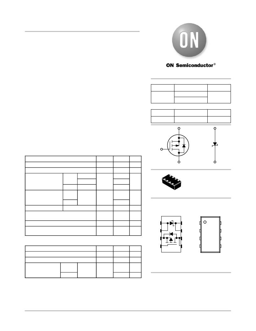
�ChipFET�
�CASE� 1206A�
�STYLE� 3�
�Pulsed� Drain� Current�
�t� p� =� 10� m� s�
�I� DM�
�?� 13�
�A�
�PIN�
�MARKING�
�Operating� Junction� and� Storage� Temperature�
�T� J� ,� T� STG�
�?� 55� to�
�150�
�°� C�
�CONNECTIONS�
�1� 8�
�DIAGRAM�
�Source� Current� (Body� Diode)�
�I� S�
�2.5�
�A�
�A�
�C�
�1�
�8�
�Lead� Temperature� for� Soldering� Purposes�
�(1/8� ″� from� case� for� 10� s)�
�SCHOTTKY� DIODE� MAXIMUM� RATINGS�
�(T� J� =� 25� °� C� unless� otherwise� noted)�
�Parameter�
�T� L�
�Symbol�
�260�
�Value�
�°� C�
�Units�
�A�
�S�
�G�
�2�
�3�
�4�
�7�
�6�
�5�
�C�
�D�
�D�
�2�
�3�
�4�
�7�
�6�
�5�
�Peak� Repetitive� Reverse� Voltage�
�DC� Blocking� Voltage�
�Average� Rectified� Steady�
�Forward� Current� State�
�T� J� =� 25� °� C�
�V� RRM�
�V� R�
�I� F�
�20�
�20�
�2.2�
�V�
�V�
�V�
�D1� =� Specific� Device� Code�
�M� =� Month� Code�
�G� =� Pb� ?� Free� Package�
�t� ≤� 5s�
�4.1�
�A�
�Stresses� exceeding� Maximum� Ratings� may� damage� the� device.� Maximum�
�Ratings� are� stress� ratings� only.� Functional� operation� above� the� Recommended�
�Operating� Conditions� is� not� implied.� Extended� exposure� to� stresses� above� the�
�Recommended� Operating� Conditions� may� affect� device� reliability.�
�1.� Surface� Mounted� on� FR4� Board� using� 1� in� sq� pad� size� (Cu� area� =� 1.127� in� sq�
�[1� oz]� including� traces).�
�ORDERING� INFORMATION�
�See� detailed� ordering� and� shipping� information� in� the� package�
�dimensions� section� on� page� 6� of� this� data� sheet.�
�?� Semiconductor� Components� Industries,� LLC,� 2008�
�November,� 2008� ?� Rev.� 4�
�1�
�Publication� Order� Number:�
�NTHD3101F/D�
�发布紧急采购,3分钟左右您将得到回复。
相关PDF资料
NTHD3102CT1G
MOSFET N/P-CH COMPL 20V CHIPFET
NTHD3133PFT3G
MOSFET P-CH SGL 20V CHIPFET
NTHD4102PT3G
MOSFET P-CH DUAL 20V CHIPFET
NTHD4401PT3G
MOSFET 2P-CH 20V 2.1A CHIPFET
NTHD4502NT1
MOSFET N-CHAN DUAL 30V CHIPFET
NTHD4508NT1G
MOSFET 2N-CH 20V 3.1A CHIPFET
NTHD4N02FT1G
MOSFET N-CH 20V 2.9A CHIPFET
NTHD4P02FT1G
MOSFET P-CH 20V 2.2A CHIPFET
相关代理商/技术参数
NTHD3102C
制造商:ONSEMI 制造商全称:ON Semiconductor 功能描述:High Efficiency DC-DC Converters
NTHD3102CT1G
功能描述:MOSFET 20V 5.5A/-4.2A Complementary RoHS:否 制造商:STMicroelectronics 晶体管极性:N-Channel 汲极/源极击穿电压:650 V 闸/源击穿电压:25 V 漏极连续电流:130 A 电阻汲极/源极 RDS(导通):0.014 Ohms 配置:Single 最大工作温度: 安装风格:Through Hole 封装 / 箱体:Max247 封装:Tube
NTHD3133PF
制造商:ONSEMI 制造商全称:ON Semiconductor 功能描述:Power MOSFET and Schottky Diode -20 V, FETKY, P-Channel, -4.4 A, with 3.7 A Schottky Barrier Diode, ChipFET?
NTHD3133PFT1G
功能描述:MOSFET PFET FETKY 20V CHIPFET RoHS:否 制造商:STMicroelectronics 晶体管极性:N-Channel 汲极/源极击穿电压:650 V 闸/源击穿电压:25 V 漏极连续电流:130 A 电阻汲极/源极 RDS(导通):0.014 Ohms 配置:Single 最大工作温度: 安装风格:Through Hole 封装 / 箱体:Max247 封装:Tube
NTHD3133PFT3G
功能描述:MOSFET -20V -4.4A P-CHANNEL W/3.7A SCHOTTKY RoHS:否 制造商:STMicroelectronics 晶体管极性:N-Channel 汲极/源极击穿电压:650 V 闸/源击穿电压:25 V 漏极连续电流:130 A 电阻汲极/源极 RDS(导通):0.014 Ohms 配置:Single 最大工作温度: 安装风格:Through Hole 封装 / 箱体:Max247 封装:Tube
NTHD4102P
制造商:ONSEMI 制造商全称:ON Semiconductor 功能描述:Power MOSFET -20 V, -4.1 A, Dual P-Channel ChipFET
NTHD4102P_05
制造商:ONSEMI 制造商全称:ON Semiconductor 功能描述:Power MOSFET -20 V, -4.1 A, Dual P-Channel ChipFET
NTHD4102PT1
功能描述:MOSFET -20V -4.1A Dual RoHS:否 制造商:STMicroelectronics 晶体管极性:N-Channel 汲极/源极击穿电压:650 V 闸/源击穿电压:25 V 漏极连续电流:130 A 电阻汲极/源极 RDS(导通):0.014 Ohms 配置:Single 最大工作温度: 安装风格:Through Hole 封装 / 箱体:Max247 封装:Tube